- 您现在的位置:买卖IC网 > Sheet目录3871 > PIC18F14K50-I/SO (Microchip Technology)IC PIC MCU FLASH 8KX16 20-SOIC
2006 Microchip Technology Inc.
Preliminary
DS70178C-page 181
dsPIC30F1010/202X
16.4
ADC Result Buffer
The ADC module contains up to 12 data output regis-
ters to store the A/D results called ADCBUF<11:0>.
The registers are 10 bits wide, but are read into differ-
ent format, 16-bit words. The buffers are read-only.
Each analog input has a corresponding data
output register.
This module DOES NOT include a circular data
buffer or FIFO. Because the conversion results may
be produced in any order, such schemes will not work
since there would be no means to determine which
data is in a specific location.
The SAR write to the buffers is synchronous to the
ADC clock. Reads from the buffers will always have
valid data assuming that the data-ready interrupt has
been processed.
If a buffer location has not been read by the software
and the SAR needs to overwrite that location, the
previous data is lost.
Reads from the result buffer pass through the data for-
matter. The 10 bits of the result data are formatted into
a 16-bit word.
16.5
Application Information
The ADC module implements a concept based on
“Conversion Pairs”. In power conversion applications,
there is a need to measure voltages and currents for
each PWM control loop. The ADC module enables the
sample and conversion process of each conversion
pair to be precisely timed relative to the PWM signals.
In a user’s application circuit, the PWM signal enables
a transistor, which allows an inductor to charge up with
current to a desired value. The longer a PWM signal is
on, the longer the inductor is charging, and therefore
the inductor current is at its maximum at the end of the
PWM signal. Often, this is the point where the user
wants to take the current and voltage measurements.
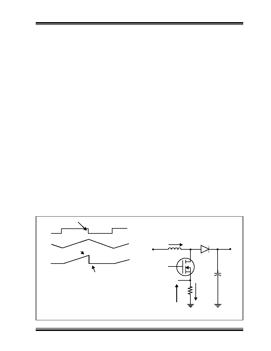
Figure 16-2 shows a typical power conversion applica-
tion (a boost converter) where the current sensing of
the inductor is done by monitoring the voltage across a
resistor in series with the power transistor that
“charges” the inductor. The significant feature of this
figure is that if the sampling of the resistor voltage
occurs slightly later than the desired sample point, the
data read will be zero. This is not acceptable in most
applications. The ADC module always samples the
analog voltages at the appointed time regardless of
whether the ADC converter is busy or not.
The Power Supply PWM module supports 2-4 indepen-
dent PWM channels as well as 2-4 trigger signals (one
per PWM generator). The user can configure these
channels to initiate an ADC conversion of a selected
input pair at the proper time in the PWM cycle. The
Power Supply PWM module also provides an addi-
tional trigger signal (Special Event Trigger), which can
be programmed to occur at a specified time during the
primary time base count cycle.
FIGURE 16-2:
APPLICATION EXAMPLE: IMPORTANCE OF PRECISE SAMPLING
X
PWM
IL
IR
X
Late sample yields
zero data
Desired sample point
Critical Edge
+VIN
IL
L
PWM
VISENSE
VOUT
COUT
+
IR
R
Measuring peak inductor current is very important
Example Boost Converter
发布紧急采购,3分钟左右您将得到回复。
相关PDF资料
PIC16F628A-I/SS
IC MCU FLASH 2KX14 EEPROM 20SSOP
PIC18LF43K22-I/PT
IC PIC MCU 8KB FLASH 44TQFP
DSPIC33FJ16MC101-I/SO
IC DSP 16BIT 16KB 20SOIC
PIC12C672-04I/SM
IC MCU OTP 2KX14 A/D 8-SOIJ
PIC12C671-04I/SM
IC MCU OTP 1KX14 A/D 8-SOIJ
PIC18F26K20-I/SO
IC PIC MCU FLASH 32KX16 28-SOIC
PIC18LF24J11-I/SO
IC PIC MCU FLASH 16K 2V 28-SOIC
DSPIC33FJ16MC102-I/SS
IC DSP 16BIT 16KB 28SSOP
相关代理商/技术参数
PIC18F14K50-I/SS
功能描述:8位微控制器 -MCU 16KB Flash 768 RAM15 I/O 10-B ADC USB 2.0
RoHS:否 制造商:Silicon Labs 核心:8051 处理器系列:C8051F39x 数据总线宽度:8 bit 最大时钟频率:50 MHz 程序存储器大小:16 KB 数据 RAM 大小:1 KB 片上 ADC:Yes 工作电源电压:1.8 V to 3.6 V 工作温度范围:- 40 C to + 105 C 封装 / 箱体:QFN-20 安装风格:SMD/SMT
PIC18F14K50T-I/SO
功能描述:8位微控制器 -MCU 16KB Flash 768 RAM15 I/O 10-B ADC USB 2.0
RoHS:否 制造商:Silicon Labs 核心:8051 处理器系列:C8051F39x 数据总线宽度:8 bit 最大时钟频率:50 MHz 程序存储器大小:16 KB 数据 RAM 大小:1 KB 片上 ADC:Yes 工作电源电压:1.8 V to 3.6 V 工作温度范围:- 40 C to + 105 C 封装 / 箱体:QFN-20 安装风格:SMD/SMT
PIC18F14K50T-I/SS
功能描述:8位微控制器 -MCU 16KB Flash 768 RAM15 I/O 10-B ADC USB 2.0
RoHS:否 制造商:Silicon Labs 核心:8051 处理器系列:C8051F39x 数据总线宽度:8 bit 最大时钟频率:50 MHz 程序存储器大小:16 KB 数据 RAM 大小:1 KB 片上 ADC:Yes 工作电源电压:1.8 V to 3.6 V 工作温度范围:- 40 C to + 105 C 封装 / 箱体:QFN-20 安装风格:SMD/SMT
PIC18F2220-E/SO
功能描述:8位微控制器 -MCU 4KB 512 RAM 25 I/O RoHS:否 制造商:Silicon Labs 核心:8051 处理器系列:C8051F39x 数据总线宽度:8 bit 最大时钟频率:50 MHz 程序存储器大小:16 KB 数据 RAM 大小:1 KB 片上 ADC:Yes 工作电源电压:1.8 V to 3.6 V 工作温度范围:- 40 C to + 105 C 封装 / 箱体:QFN-20 安装风格:SMD/SMT
PIC18F2220-E/SP
功能描述:8位微控制器 -MCU 4KB 512 RAM 25 I/O RoHS:否 制造商:Silicon Labs 核心:8051 处理器系列:C8051F39x 数据总线宽度:8 bit 最大时钟频率:50 MHz 程序存储器大小:16 KB 数据 RAM 大小:1 KB 片上 ADC:Yes 工作电源电压:1.8 V to 3.6 V 工作温度范围:- 40 C to + 105 C 封装 / 箱体:QFN-20 安装风格:SMD/SMT
PIC18F2220-I/SO
功能描述:8位微控制器 -MCU 4KB 512 RAM 25 I/O RoHS:否 制造商:Silicon Labs 核心:8051 处理器系列:C8051F39x 数据总线宽度:8 bit 最大时钟频率:50 MHz 程序存储器大小:16 KB 数据 RAM 大小:1 KB 片上 ADC:Yes 工作电源电压:1.8 V to 3.6 V 工作温度范围:- 40 C to + 105 C 封装 / 箱体:QFN-20 安装风格:SMD/SMT
PIC18F2220-I/SO
制造商:Microchip Technology Inc 功能描述:IC 8BIT FLASH MCU 18F2220 SOIC28
PIC18F2220-I/SOC03
制造商:Microchip Technology Inc 功能描述: